For the circuit shown, find the b-parameter j6 N ell -j3 Q


Q: Give examples for the following: A.) 1 example of DC analysis of darlington pair solved problem.…
A: A Darlington pair is designed by using the combination of two BJTs connected in such a way that the…
Q: Obtain the transfer function X,(s)/X,(s) of the mechanical system shown in Figure- Q3(a) and the…
A:
Q: 5. A discrete-time signal x[n] is shown in Figure below. Sketch and label each of the following…
A: To sketch the discrete time signal
Q: NC= 16
A: A transfer function of a system is a mathematical expression of the system and is defined as the…
Q: Q4) For the circuit shown, Find the output voltage and sketch it when the input voltage is 1v and…
A: The above circuit represents the op-amp Integrator. According to the given Input Waveform it…
Q: (b) Draw the signal flow graph of a system represented by the following block diagram and find C/R…
A: In this question, Find the transfer function of the given block diagram using the Mason gain…
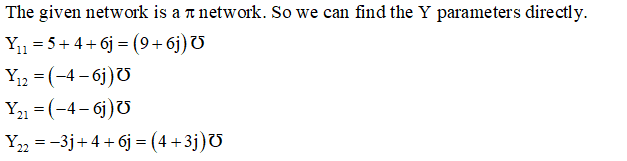
Q: Given the circuit in figure below, find the z parameter. 1. Is 32
A:
Q: 2) Using a FamH nductor design (and draw belw) a Ist order passive high ass A Her with a cutoff…
A:
Q: ) Define the function of opamp circuit given below. DetermineV, for the circuit shown below. 2K 3K…
A:
Q: Draw the graph between transconductance and Vgs-Vth with W/L constant. also the graph between…
A: MOSFET(Metal Oxide Semiconductor field effect Transistor) is three terminal electronic device.…
Q: True and False (correct the false) 1- Class -A: the output stage conducts for a full 360° (a full…
A: Dear student as per our guidelines we are supposed to solve only one question in which it should…
Q: according to the figure below; a) y[n] = 3r[n]+2g[n] plot signal. b) y[n]δ[n-4] and y[n]δ[n+2] Find…
A:
Q: G3($) CCSI てS) GCS) Gz(S) G4 CS) HIS)
A: As we have to calculate the overall transfer function of this block diagram So we have two ways to…
Q: Q) Given a discrete signal x[n] = (4, 5) what is DFT[x[n] Select one: • a. [-1 9] O b. = [9 -1)…
A: Givenxn=4,5
Q: Q) Draw and Design an op amp circuit whose input is Vs, output is Vo, and transfer characteristic is…
A:
Q: Plot the output signal showing the proper relationship to the input signal in the following circuit,…
A: Consider the output reference voltage is determined by the two resistances as, VREF=R2R1+R2±14…
Q: Q1: A discrete-time signal is shown in the Figure below. Sketch and label each of the following…
A: Given signal is -
Q: 4/ by using signal flow graph determin the trans fer function of CYz/Ri) for the figer. -H2 G4 Ri 67…
A: Signal flow graph is also known as Mason's graph. It is specialized graph or directed graph in which…
Q: Q- 2: Suppose you are designing a Mathematical Calculator. You need Logarithmic and Anti logarithmic…
A:
Q: Q2: Draw the output waveforms (S, X, and Y) for the below sequential circuit by assuming the…
A:
Q: Find the operating point and small signal components of the nonlinear 3-T element. Vs =-6V, Isı =…
A: Given, Vs=V1=-6VIs1=I2=3AIs2=07cos5(t)i1=12V1+12V2V2=3i22 + 2i1V1
Q: In order for a méasüring instrufffent to relationship with the circuit output resistance Rs: Rin >>…
A: When the output of the some circuit has to be connected to some measuring instrument , impedance…
Q: Q3) Draw the output waveform for the circuit in figure below. Assume that +Vout(max) = +10 V and -…
A: By knowing the property of zener diode and operation amplifier we need to plot output waveform of…
Q: (c) Determine the transfer function of the system as shown in Figure block diagram reduction method.…
A: In this question, We need to determine the transfer function using the block diagram reduction…
Q: For the following amplifier small signal equivalent circuit, Rin is Rsi Select one: O a. ww R1||R2…
A: We need to select correct option for input impedance for given circuit
Q: Reduce the block diagram shown in the Figure below, and find the transfer junction C(s)/R(s). G4…
A:
Q: Q2) Draw the output waveforms on top of the input waveforms for the circuits below. For all circuits…
A: In this question, We need to draw the output voltage waveform of the given op amplifier. We are…
Q: H.W 1: - Draw the signal Flow Graph for the following set of equations V1 = 5V2 + 4V; V2 = 2V1 +…
A:
Q: 2. For the inverting OPAMP circuit given below compute the transfer function Vi R1 C1 HH R2 Vo(S) VI…
A:
Q: Obtain the transfer function (Eo(s)/Ei(s)) of the op-amp circuit R1 R1 ww A C eo R2 ej + B.
A: Fig: Given circuit
Q: 2) Represent the following set of equations by a signal flow graph and the overall gain relating x5…
A: Represent the following set of equations by a signal flow graph and the overall gain x₂ = ax₁ + fx₂…
Q: G2 R H1
A: We need to find out transfer function for given system
Q: b) Convert the block diagram of FigureQ2 to a signal flow graph and find transfer function using…
A: Here there is Forward path gain is given by F1=1s1s1s=1s3
Q: For the system below 1) find transfer function (output/input) 2) analyze model by using proper test…
A: TO FIND THE TRANSFER FUNCTION
Q: 2.Implement the following block diagram with unit step input signal, show the output on scop : R(s)…
A: The reduced block diagram is shown below:
Q: 1. Construct a state diagram for a Mealy-type circuit with input v and output g that is to recognize…
A: A state diagram, in particular, displays how a single object in a system reacts to a sequence of…
Q: Determine the error ratio of the block diagram below using a) Block Diagram Reduction, and b)…
A:
Q: Q) Draw and Design an op-amp circuit whose input is Vs, output is Vo, and transfer characteristic is…
A:
Q: Q2: For the below signal flow graph find the correct answer and verfiy why in details. The state…
A:
Q: 4. ( signal flow graph in each step. Show step by step and complete solution. Determine the output C…
A: This block diagram shown in fig. Can be solved by signal flow graph with help of Mason’s Gain…
Q: نقطة واحدة If the following data-input waveforms applied to the comparator, the output in relation…
A:
Q: Implement the following functions using Op-Amps:
A:
Q: In the figure shown below find the value of R1 and R2 if the output response be Vo= 3 Vy – 5 Vx
A: Let the voltages at node x be V1 and the voltage at node y be V2. Given VX voltage is applied at…
Q: You have a 100 mV signal in the frequency range 600 Hz to 700 Hz with which you want to drive a 200N…
A: Noise is a consistent issue in power-supply plan. While there are FCC limits on the electromagnetic…
Q: A boost converter is a dc-to-de switched power supply in which the voltage output is larger than the…
A:
Q: Given the shown circuit and its feedback block diagram, find the transfer function in the block B3.…
A:
Q: G2 R Gi
A: We need to find out the transfer function for given system
Q: (0.1 Design a adder circuit using Op-Amp to obtain an output expresSion Vo = .5V2 + 20V3). Where V,,…
A:
Q: A discrete-time signal is shown in Figure below. Sketch and label carefully each of the following…
A: Signal- Signal is a physical phenomenon that contain information. Mathematically, signal is defined…


Step by step
Solved in 2 steps with 2 images


- on to Electronic Analysis and Design-C urses / Introduction to Electronic Analysis and Design - C The difference between Vcs and vGs is Select one: a. The first is ac and the second is de b. The first is ac and the second is ac + de c. The first is de and the second is ac + dc d. The first is de and the second is acDraw basic internal architecture of IC 7492 and design divide by 9 counter Sng IC 7492.4- For an operational amplifier circuit below. Draw the input and output waveforms if Vin is sine wave with 10 mV,R₁ = 10 KM, and R₂ = 100 KM. VI R₂ www PO
- Sketch the output voltage waveform for each op armp circuits given below. Given the maximum outputvoltage for the op-armp is Vomax = +10 v and Vomin = -10 v.Use input voltage for all circuit as shown. Also use V2 = 4.7 V for D1 and D2. V. 0 -5V- -5V D1 Kt 1K 1K D2 V1 V2There is a sinuoidal input signal in the Op-Amp application circuit below. Draw the signal waveforms on A1 and A2 points by determining y-axis values, as well. (R3=1.5kΩ, C1=10nF, R1=R2=10kΩ).the picture attched is of a buck converters switching voltages acros the inductor. the inductor has a value of 10mH If the switching frequancy is 10khz's, how bigger load in Ohms will cause the converter to go into DCM and what size capacitor will be required to make this converter have a output ripple of 1%
- A computer manufacturing company has approached you to assist it to design a summer circuit for its new type of computers. You are provided with resistors R1, R2, R3, R4 and a feedback resistor Rf. Design and draw the summer circuitii. Derive the formula for the output voltage Vo of the summer circuitBkcBZYhc850ZmX4-RzV7i6yWprtMcdra5me-w_Og/formResponse The DAC with inputs and outputs shown in figure below, the fault in the circuit is in note (all the values is in approximate range ) RF R1 200 120k U1 R2 60k R3 741 30k R4 15k - 13.2 mV - 15.6 mV - 29.9 mV -65.6 mV -79.9 mV - 82.2 mV - 96.5 mV R1 O R2 0000 0010 0100 0110 000 1001 1010 1011 1101 1110 III 0000Vi is a sinusoid signal of 8 Vp-p and f = 1 kHz. Vref = 2 V and V1 = 5 V and V2 = -1V. Assume that V1 is connected to pin7 of op-amp 741 and V2 is connected to pin 4. The output Vo will be, * V1 Vo 741 Vret O A square wave of 6 Vp-p, 1 kHz A rectangular wave of 6 Vp-p, 1 kHz A triangular wave of 6 Vp-p, 1 kHz A sinusoid wave of 8 Vp-p, 1 kHz A rectangular wave of 4 Vp-p, 1 kHz A square wave of 8 Vp-p, 1 kHz A sawtooth wave of 6 Vp-p, 1 kHz O A sinusoid wave of 6 Vp-p, 1 kHz
- How many op-amps are required to implement this equation? Rf Vz R₁ R₂ R₁ R₂ V₁ (V₁) R₂ R₁ O 2 3 04Design an op-amp circuit that meets the following specifications. Your design can be done with one or two op-amps. Your instructor may give you a different design. Note: Show all work. Draw a schematic of your design and label component values and op-amp pin numbers. a. The op-amp circuit must have a non-inverting overall voltage gain that is adjustable from +3 to +12. The circuit has a 47 k load resistor connected from the last op-amp's output terminal to ground. b. c. The circuit input resistance must be ≥ 50 kn. Your design is limited to a maximum of two op-amps and seven resistors, one of which is a variable 100 k resistor (potentiometer). The potentiometer resistance is 0 22 when adjusted to one extreme of its range and 100 k at the other extreme. d. When the potentiometer is adjusted to one extreme position the overall circuit voltage gain should be +3. When the variable resistor is adjusted to its other extreme position the overall circuit voltage gain should be +12.Design and draw three-bits subtraction respectively using only Half Subtractor. Differentiate between analysis and design framework of combinational circuits.