
Videos
In the circuit in Figure P14.38, the offset voltage of each op−amp is ±3 mV.
(a) Determine the possible range in output voltages
(b) Repeat part (a) for
(d) Design offset voltage compensation circuit(s) to adjust both
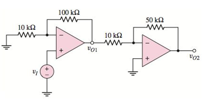
Figure P14.38
(a)
The possible range in output voltages
Answer to Problem 14.38P
The possible range in output voltages
Explanation of Solution
Given:
Given circuit:

Given offset voltage,
Calculation:
Now the input voltage is,
For the first op-amp which is a non-inverting amplifier, the gain is,
The possible range in the output voltage
For the second op-amp which is an inverting amplifier, the gain is,
Substitute
The possible range in the output voltage
Given
Above circuit can be represented as below

From equation
From equation (2) , the possible range in the output voltage
(b)
The possible range in output voltages
Answer to Problem 14.38P
The possible range in output voltages
Explanation of Solution
Given:
Given circuit:

Given offset voltage,
Calculation:
Now the input voltage is,
For the first op-amp which is a non-inverting amplifier, the gain is,
The possible range in the output voltage
For the second op-amp which is an inverting amplifier, the gain is,
Substitute
The possible range in the output voltage
Given
Above circuit can be represented as below

From equation
From equation (2), the possible range in the output voltage
(c)
The possible range in output voltages
Answer to Problem 14.38P
The possible range in output voltages
Explanation of Solution
Given:
Given circuit:

Given offset voltage,
The given value is
Calculation:
Now the input voltage is,
For the first op-amp which is a non-inverting amplifier, the gain is,
The possible range in the output voltage
For the second op-amp which is an inverting amplifier, the gain is,
Substitute
The possible range in the output voltage
Given
Above circuit can be represented as below

From equation
From equation (2) , the possible range in the output voltage
(d)
To design: The offset voltage compensation circuit(s) to adjust both
Answer to Problem 14.38P
The offset voltage compensation circuit is shown in Figure 1.
Explanation of Solution
Given:
Given circuit:
Given offset voltage,
Calculation:
The output voltages for the given input voltage
The adjusting compensation circuit for the range of output voltages as well as input voltage is shown below.
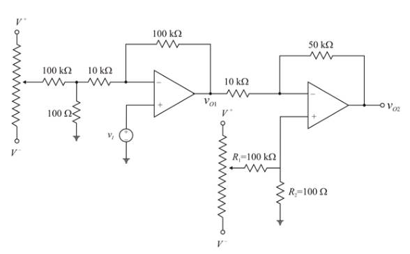
Figure 1
Want to see more full solutions like this?
Chapter 14 Solutions
Microelectronics: Circuit Analysis and Design


- c) A buck converter with constant frequency peak current mode control has Vs = 28V, V = 20V, L = 301uH, fs = 100 kHz. Find the ramp slop for the optimum compensation and the peak compensation voltage. %3Darrow_forwardthe way of working for boost dc-to-dc converter.arrow_forwardA signal generator having a source resistance of 50 2 is set to generate a 1 kHz sinewave. Open circuit terminal voltage is 10 V peak-to-peak. Connecting a capacitor. across the terminals reduces the voltage to 8 V peak-to-peak. The value of this capacitor is -HF. (Round off to 2 decimal places).arrow_forward
- A 10-Ohm fully resistive load system will be fed from a photovoltaic (PV) module. Load (converter output) voltage 12 V DC is required. But the PV output is DC 18 Volt. Buck type DC/DC converter design is required between load and PV. For this j-converter, the inductor current must be continuous and the fluctuation rate of the load voltage must be at most 0.5%. The lowest switching frequency is 40 kHz; A) What is the lowest Capacitor value (microF) that meets the design conditions for the output capacitor ? B) What is the RMS value of the inductor current (A) ? C) What is the average value of the inductor current (A) ?D) What is the inductance value (microH) that meets the design prerequisites?E) What is the lowest inductance value to be calculated (microH) ?F) What is the operating ratio of the circuit (Duty) ? Please answer D;e;farrow_forwardA 10-Ohm fully resistive load system will be fed from a photovoltaic (PV) module. Load (converter output) voltage 12 V DC is required. But the PV output is DC 18 Volt. Buck type DC/DC converter design is required between load and PV. For this j-converter, the inductor current must be continuous and the fluctuation rate of the load voltage must be at most 0.5%. The lowest switching frequency is 40 kHz; A) What is the lowest Capacitor value (microF) that meets the design conditions for the output capacitor ? B) What is the RMS value of the inductor current (A) ? C) What is the average value of the inductor current (A) ?D) What is the inductance value (microH) that meets the design prerequisites?E) What is the lowest inductance value to be calculated (microH) ?F) What is the operating ratio of the circuit (Duty) ?arrow_forwardIn the full-wave rectifier circuit of figure , the transformer has a turns ratio of 1:2. The transformer primary winding is connected across an AC source of 23oV (rms), 50 Hz. The load resistor is 50ohms. For this circuit, determine the peak-to- peak ripple in the output voltage * Di V2 = VmSin cot Vs (N Vo + V3 = VmSin ot D2 Full-wave rectifier- Circuit operation during positive half cycle 460 V 207 V 325.3 V O None of the above ell ellarrow_forward
- A single-phase full-wave converter in the figure below is supplied with a 120-V, 60-Hz source. The load is highly inductive and the load current is continuous and free of ripples. The electromotive force is neglected (E 0) and the resistance has a value of R = 10 Q. The delay angle is equal to 31.8°. The average output current is 9.18A and the nth harmonic component is expressed as below. The harmonic factor (known as THD) would be equal to: R 2. vZ.1. Ir = Vo n. T +Yi, = I, E Select one: O a. 58.3% Ob. 48.3% O C. 78.3% Od. 68.3%arrow_forwardA fully controlled, single-phase bridge rectifier is powered from an ideal 220V, 50Hz source. The rectifier is triggered with a trigger angle of 60 degrees and provides a smooth current of 50A to the load at the output. According to this: a) Draw the waveform of the output voltage in scale and calculate the average value of the output voltage. Combine the average voltage signal with the output voltage wave signal. Show on the same figure. b) Draw the waveforms of the thyristor currents, the gap diode current and the current drawn from the source in scale. c) Calculate the value of the filter inductance used at the output when the ripple in the load current is 3A. (Do the operations by showing the output voltage shapes and areas on the figure. The answers should be in the system and order in the solved examples.)arrow_forwardInput voltage of a boost converter 80 V, output voltage 140 V and switchingits frequency is 20 kHz. The converter efficiency is known to be 95%.a) Continuous conduction (current) in operation when the load resistance changes between 14 - 20ohmThe lowest inductance (L) value and output that should be used to maintain the operation.the peak-to-peak value of the voltage ripple should be used to be 2% of the output voltage.Calculate the capacitor's capacity (C).arrow_forward
- Question No. 2 a Inan experiment the voltage required for the device is 9V dc but unfortunately the transformer avai lable is of 220-6 V dc. Design a circuit which can power the device (use only methods that we have studied excluding Zener diode) b. Explain the behavior of the foll owing circuits if the input signal is triangular wave of peak voltage 5V and the biasing battery of 3V 4-arrow_forwardWhat is the maximum dc voltage you could expect to obtain from a transformer with an 18 Vrms secondary using a bridge rectifier circuit with a filter capacitor? in your own wordsarrow_forwardA single-phase full-wave converter in the figure below is supplied with a 120-V, 60-Hz source. The load is highly inductive and the load current is continuous and free of ripples. The electromotive force is neglected (E = 0) and the resistance has a value of R = 10 2. The average output voltage is 85% of the maximum possible average output voltage. The delay angle would be equal to: Select one: 81.8° O b. 31.8° O c 67.8° O d. 51.8° AT₁ AT, R L +7=4₂ Warrow_forward
 Introductory Circuit Analysis (13th Edition)Electrical EngineeringISBN:9780133923605Author:Robert L. BoylestadPublisher:PEARSON
 Delmar's Standard Textbook Of ElectricityElectrical EngineeringISBN:9781337900348Author:Stephen L. HermanPublisher:Cengage Learning
 Programmable Logic ControllersElectrical EngineeringISBN:9780073373843Author:Frank D. PetruzellaPublisher:McGraw-Hill Education
 Fundamentals of Electric CircuitsElectrical EngineeringISBN:9780078028229Author:Charles K Alexander, Matthew SadikuPublisher:McGraw-Hill Education
 Electric Circuits. (11th Edition)Electrical EngineeringISBN:9780134746968Author:James W. Nilsson, Susan RiedelPublisher:PEARSON
 Engineering ElectromagneticsElectrical EngineeringISBN:9780078028151Author:Hayt, William H. (william Hart), Jr, BUCK, John A.Publisher:Mcgraw-hill Education,