
Videos
a.
Worst case output voltage for given circuit.
a.
Answer to Problem 14.55P
The worst case output voltage is
Explanation of Solution
Given:
The given circuit is shown below.
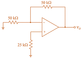
Input offset voltage
Average input bias current
Input offset current
Calculation:
On applying
For given circuit
For an op-amp
Then,
Now, KCL at input nodes:
For op-amp circuit
Now, output voltage due to input bias current and input offset current is,
Due to offset voltage,
From equation (1)
So, the worst case output voltage for the circuit will be,
b.
Worst case output voltage for given circuit.
b.
Answer to Problem 14.55P
The worst case output voltage is
Explanation of Solution
Given:
The given circuit is shown below.
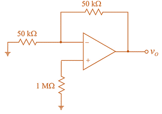
Input offset voltage
Average input bias current
Input offset current
Calculation:
Consider the circuit shwon below.
Apply KCL at non-inverting terminal
For op-amp
So,
Now, KCL at inverting terminal,
Putting
As,
And
Adding (4) and (5)
From (4)
For
For
For the circuit
If offset voltage is negative, then from (1)
Let
Putting
So, the worst case output voltage for circuit is
Want to see more full solutions like this?
Chapter 14 Solutions
Microelectronics: Circuit Analysis and Design


- Op amp and diodes are ideal. Derive Vout and sketch the transfer curve of Vin vs Vout. Please show complete solution.arrow_forwardExplain virtual short circuit of opamp.arrow_forwardGive reasons for the following:(i) The gain of the Opamp rolls off after a certain frequency is reached.(ii) The Output offset voltage generated by the input bias current is always greater than that generated by the input offset current.arrow_forward
- The input voltage for an Op-Amp series regulator is 12v,, if the non inverting input of the op-Amp is connected to 3 series diodes instead of Zener one . a) Design the the op-amp feedback resistors to give 6.5V fixed o/p voltage b) Determine the line regulation in both % and in %/V. if the input voltage increased by 3V leading to o/p voltage increase of 0.05arrow_forwardYou are tasked to look for a converter circuit design that has the specifications tabulated in Table I. The aim is to produce an output voltage of 20 V which can be used to drive a load of 120 W. The converter must operate in CCM. Table I: Design Specifications Values 35 V Design Parameters Input voltage Switching frequency Output current ripple Output voltage ripple 60 kHz 5 % 1 % a) Sketch the final converter and label all parameter valuesarrow_forwardQ2/Explan the method to compensation of bias current, offset voltage,Offset current and maximum output voltage swing of op-amp.arrow_forward
- Draw the circuit of OP AMP controlled Series regulator and explain how its maintain output voltage constantarrow_forwardIn the figure a series voltage regulator circuit is shown. Design the value of R1, R2 and R of the voltage regulator when an 8 V Zener diode is used to maintain a regulated output voltage, VL, of 20 V. Assume that the unregulated input varies between 18 V and 22 V, and that the Op-Amp is ideal. The minimum Zener current needed to keep it in breakdown is 10 mA.(need only handwritten solution .otherwise downvote.)arrow_forwardIn the circuit in figure, what is Voc? Zth? Rl? Pmax?arrow_forward
- Using any number of Op-Amps, design multistage amplifier to amplify input Ac signal with 0.01V amplitude, the expected output voltage would have 4V amplitude. The input signal frequency = 10 KHz. Assume gain bandwidth product of Op-Amp = 1 MHzarrow_forwardc) A buck converter with constant frequency peak current mode control has Vs = 28V, V = 20V, L = 301uH, fs = 100 kHz. Find the ramp slop for the optimum compensation and the peak compensation voltage. %3Darrow_forwardQI/Explan the method to compensation of bias current, offset voltage,0ffset current and maximum output voltage swing of op-amp.arrow_forward
 Electricity for Refrigeration, Heating, and Air C...Mechanical EngineeringISBN:9781337399128Author:Russell E. SmithPublisher:Cengage Learning