
Videos
For the transistor in the circuit in Figure P6.26, the parameters are
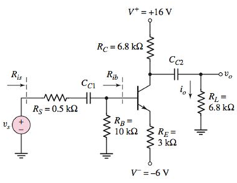
Figure P6.26
(a)
The quiescent
Answer to Problem 6.26P
The quiescent
Explanation of Solution
Given:
The current gain
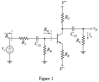
The circuit for
The circuit parameters are written below.
Concept used:
The expression for quiescent collector current is written below.
Calculation:
Apply dc analysis and KVL in base emitter loop.
Substitute
Substitute
Therefore, the quiescent collector current
Apply KVL in base collector loop.
Substitute
Therefore, the
Conclusion:
Thus, the quiescent
(b)
The hybrid
Answer to Problem 6.26P
The transconductance
Explanation of Solution
Concept used:
The expression for transconductance
The expression for diffusion resistance
The expression for output resistance
Calculation:
Substitute
Therefore, the transconductance
Substitute
Therefore, the diffusion resistance
Substitute
Therefore, the output resistance
Conclusion:
Thus, the transconductance
(c)
The small signal voltage gain
Answer to Problem 6.26P
The small signal voltage gain
Explanation of Solution
Concept used:
The expression for small signal voltage gain
The expression for small signal current gain
Calculation:
The input resistance
Substitute
Therefore, the small signal voltage gain
Substitute
Therefore, the small signal current gain
Conclusion:
Thus, the small signal voltage gain
(d)
The input resistance
Answer to Problem 6.26P
The input resistance
Explanation of Solution
Concept used:
The expression for input resistance
The expression for input resistance
Calculation:
Substitute
Therefore, the input resistance
Substitute
Therefore, the input resistance
Conclusion:
Thus, the input resistance
(e)
The small signal voltage gain
Answer to Problem 6.26P
The small signal voltage gain
Explanation of Solution
Concept used:
The expression for small signal voltage gain
Calculation:
Substitute
Therefore, the small signal voltage gain
Since, small signal current gain is independent of source resistance, so it is same as obtained in part (c).
Therefore, the small signal current gain
Conclusion:
Thus, the small signal voltage gain
Want to see more full solutions like this?
Chapter 6 Solutions
Microelectronics: Circuit Analysis and Design


- Draw Zener regulator circuit to obtain regulated DC voltage 6.8 V. Considering input DC voltage in the range from 10V to 30V. Consider load resistance of 10KΩ.arrow_forward4. a) Determine the output waveform for the following circuit. b) Repeat with the B input held LOW c) Repeat with B held HIGH A 4. 1 0. I Time 1 0.arrow_forwardR +Vcc -Vcc C Vout R R a. Quantify how the resistors and the capacitor influence the output voltage of the circuit, Vout. What are the upper and lower limits of Vc? b. Howlong does it take for the capacitor to be charged from minimum to maximum voltage and vice versa?arrow_forward
- 5. Determine Leq at terminal a-b the circuit below. Ans.7.778 mH 10 mH 60 mH 25 mH 20 mH a o o b ele 30 mHarrow_forwardthis is electric circuit questin ...plz solve it early .plz solve earlyarrow_forwardb.com Snubbers are an essential part of power electronics to protect the active devices. Design a snubber circuit and explain how thyristors are protected against high di/dt and high dv/dt.arrow_forward
- Q2. For the circuit shown below, sketch i, & Vo 60 a. Find the conduction angle of the thyristor. b. Find the average output voltage V. R-6.50 f- Go Hz = 27AL = 120x17X10 = 6.4092 075 LO = RrjX= Vo L-17mH 6.5+j6.469=9.128 (44595 075 75V( Es 24 Vm A earrow_forwardPlease answer both subpart for like this please Asap for like..arrow_forwardBoost Converter Design A boost converter is required to have an output voltage of 8 V and supply a load current of 1 A. The input voltage varies from 2.7 to 4.2 V. A control circuit adjusts the duty ratio to keep the output voltage constant. Select the switching frequency. Determine a value for the inductor such that the variation in inductor current is no more than 40 percent of the average inductor current for all operating conditions. Determine a value of an ideal capacitor such that the output voltage ripple is no more than 2 percent. Determine the maximum capacitor equivalent series resistance for a 2 percent ripple.arrow_forward
 Introductory Circuit Analysis (13th Edition)Electrical EngineeringISBN:9780133923605Author:Robert L. BoylestadPublisher:PEARSON
 Delmar's Standard Textbook Of ElectricityElectrical EngineeringISBN:9781337900348Author:Stephen L. HermanPublisher:Cengage Learning
 Programmable Logic ControllersElectrical EngineeringISBN:9780073373843Author:Frank D. PetruzellaPublisher:McGraw-Hill Education
 Fundamentals of Electric CircuitsElectrical EngineeringISBN:9780078028229Author:Charles K Alexander, Matthew SadikuPublisher:McGraw-Hill Education
 Electric Circuits. (11th Edition)Electrical EngineeringISBN:9780134746968Author:James W. Nilsson, Susan RiedelPublisher:PEARSON
 Engineering ElectromagneticsElectrical EngineeringISBN:9780078028151Author:Hayt, William H. (william Hart), Jr, BUCK, John A.Publisher:Mcgraw-hill Education,