
Videos
a.
The value of the resistor R1 and R2 in a way that the dc value of the output voltage is 0.
a.
Answer to Problem 11.89P
The value of the resistances are:
Explanation of Solution
Given:
The circuit is given as:

The circuit parameters:
The drain current of
Considering the expression for drain current of
Hence, the value of the resistor
Evaluating the value of source gate voltage of
Considering the expression for the drain current of
Hence, the value of the resistor
b.
To sketch: The small signal equivalent circuit and then find the small signal transistor parameters.
b.
Explanation of Solution
Given:
The circuit is given as:

The circuit parameters:
Evaluating the value of trans-conductance
Substituting
Evaluating the value of trans-conductance of
Evaluating the value of the resistor
Evaluating the value of the resistor
c.
The small signal voltage gain.
c.
Answer to Problem 11.89P
The small signal gain of the circuit is -15.25V/V.
Explanation of Solution
Given:
The circuit is given as:
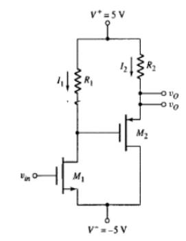
The circuit parameters:
Drawing the small signal equivalent model of the circuit:
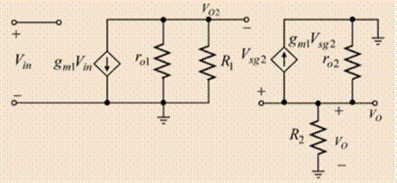
Applying nodal analysis at the input node:
Referring to the above diagram:
Applying the nodal analysis at the output node:
Hence, the small signal gain of the circuit is -15.25V/V.
d.
The output resistance.
d.
Answer to Problem 11.89P
The value of the output resistance is
Explanation of Solution
Given:
The circuit is given as:

The circuit parameters:
Evaluating the output resistance
Substituting
Hence, the value of the output resistance is
Want to see more full solutions like this?
Chapter 11 Solutions
Microelectronics: Circuit Analysis and Design


- Small amount of space it takes on a chip O All of the above 7. The main types of field effect transistor are O BJT and FET O UJT and FET O JFET and MOSFET O None of the above 9.The arrow on the symbol of MOSFET indicat that it is a N-channel MOSFET the direction of electrons O the direction of conventional current flow O that it is a P-channel MOSFETarrow_forward8. The circuit shown below is a small sine wave signal with average zero andtransistor ß =98Find the value of R(E) to establish a dc emitter current of about 0.8 mAarrow_forwardThe term "Bipolar" in Bipolar Junction Transistor (BJT) refers to 5 Ja) Two junctions c) Two polarity carriers (electrons & holes) b) Two Diodes d) Two resistances negative of dinda b' nositivoarrow_forward
- A stabilization circuit has a stability factor of 0.04 and an internal resistance of 5 2. The unstabilized voltage can vary between 75 and 100 V, and the load current can vary from 40 to 80 mA. Determine the maximum and minimum values for the stabilized load voltage.arrow_forwardFrom the circuit below, determine the output peak voltage Vm ? Np:Ns 6:1 Vp 120 Vac out 60 Hz DA R = 200 2 O Ovpeak O 169.71Vpeak O 28.28Vpeak O 1018.23Vpeakarrow_forwardSolve for Collector Resistance (RC)arrow_forward
- If the circuit shown in Figure #1 had a 10 kΩ resistor connected as a load resistor, RL and an input signal is applied to the base of the transistor through the coupling capacitor C1, with an amplitude of 22 mVpp at a frequency of 1 kHz. Determine the new voltage gain AV and the output voltage VOUT. Is the output signal clipped?arrow_forwardwe can see the following signal at which point of the modulator? 6 A Modulating signal D Carrier AM output В B D None of these C Cor D A This signal will never be presented in this modulatorarrow_forward4. An RC filter stage (R = 33 0, C = 120 HF) is used to filter a signal of 24 V dc with 2 V rms operating from a full wave rectifier. Calculate the percentage ripple at the output of the RC Section for a 100-mA load. Also calculate the ripple of the filtered signal applied to the RC stage. *****END*****arrow_forward
- 4. An RC filter stage (R = 33 02, C = 120 µF) is used to filter a signal of 24 V dc with 2 V rms operating from a full wave rectifier. Calculate the percentage ripple at the output of the RC Section for a 100-mA load. Also calculate the ripple of the filtered signal applied to the RC stage.arrow_forwardA. Find the value of Ibq B. Find the value of Rf C. Find the value of (Re) tarrow_forwardA boost regulator has L=0.15 mH and C=0.11 mF with a duty cycle of 0.66 at a switching frequency of 50 kHz. The average load current is la=0.5A. The maximum ripple output voltage is: Select one: a. None of these b. 1.6V C. 2.6V d. 0.6Varrow_forward
 Introductory Circuit Analysis (13th Edition)Electrical EngineeringISBN:9780133923605Author:Robert L. BoylestadPublisher:PEARSON
 Delmar's Standard Textbook Of ElectricityElectrical EngineeringISBN:9781337900348Author:Stephen L. HermanPublisher:Cengage Learning
 Programmable Logic ControllersElectrical EngineeringISBN:9780073373843Author:Frank D. PetruzellaPublisher:McGraw-Hill Education
 Fundamentals of Electric CircuitsElectrical EngineeringISBN:9780078028229Author:Charles K Alexander, Matthew SadikuPublisher:McGraw-Hill Education
 Electric Circuits. (11th Edition)Electrical EngineeringISBN:9780134746968Author:James W. Nilsson, Susan RiedelPublisher:PEARSON
 Engineering ElectromagneticsElectrical EngineeringISBN:9780078028151Author:Hayt, William H. (william Hart), Jr, BUCK, John A.Publisher:Mcgraw-hill Education,