
Videos
The transistor parameters for the circuit in Figure
a.
To design: The circuit for the given parameters.
Answer to Problem D11.105DP
The design of the given circuit is shown in Figure 2.
Explanation of Solution
Given:
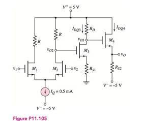
The given circuit is shown below.
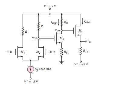
Figure 1
Calculation:
Consider the differential circuit part,
The circuit is symmetrical because currents divides between both MOSFETs. Now consider one by one part of the circuit.
Now find
Now find
Now calculate
Now the design is shown below.
Figure 2
b.
The differential-mode gains.
Answer to Problem D11.105DP
Explanation of Solution
Given:
The given circuit is shown below.

Calculation:
Consider the
Put the calculated values in above equation,
Now,
Now find,
Put the values in
c.
The common-mode voltage gains and
Answer to Problem D11.105DP
Explanation of Solution
Given:
The given circuit is shown below.

Calculation:
Consider the
Hence the
Want to see more full solutions like this?
Chapter 11 Solutions
Microelectronics: Circuit Analysis and Design


- PLease find the Transconductance value of the Transistors below a. μnCox = 250 μA/V², W/L=10, Vgs=2V and Vth=0.7V b. μnCox = 250 μA/V², W/L=10 and Id=1 mA c. Id= 1 mA, Vgs=1.7 V and Vth=0.5Varrow_forwardShown below is a PNP CE amplifier with large AC coupling capacitors Cx and Cy with: Q1 has the following : VeB,Q = 0.7V, Vec,SAT = 0.2V, PNP Q1 VA → 00 Cx Rin Rx vin vout B = 100. Vr = 0.026V| 5k 430k Ry Rz 5k 5k Find Ico, VEc,Q, 9m1,rn1, Gm, Ro, Ayarrow_forward294 227 The op amp in the crout in the figure is ideal. (Figure 1) The de signal source has a value of 860 mV Figure 1630 ww 24301 w ISV 15 V 102> Part A Find the Thevenin voltage of the equivalent circuit (Eigure 2) with respect to the output terminals a, b Express your answer with the appropriate units. Vn Submit Part RD- -11.55 Submit Part C X Incorrect, Try Again: 2 attempts remaining 4 Previous Answers Request Answer Find the Thevenin resistance of the equivalent circuit with respect to the output terminals a, b, Express your answer with the appropriate units Value V Value C 4 n What is the output resistance of the invertingamp Express your answer with the appropriate units. Units 03 ? ? Units PPearson ?arrow_forward
- In the circuit of the following figure VBB = 2V, RB = 100kΩ, RC = 1kΩ, VCC = 10V. Determine:a) What is the value of the base current? What is the voltage across the base resistor?b) the collector current, if βdc = 100? What is the VCE voltage?c) the collector current, if βdc = 200? What is the VCE voltage?d) Compare the results of parts b and carrow_forwardA)Find the expression that gives the voltage transfer function k for V0 = k.Vs for the circuit given in the figure. B) Bölüm A'da elde ettiğiniz ifade için 1 kohm için tüm direnç değerlerini alarak k ifadesini hesaplayın.arrow_forwardA certain non-linear device has the following output current expression: + V1 11 1₂ = loe V₁/VT (1 – e-V₂/VT) - = Non Linear BLACK BOX Answer: 124 Find the linear small signal approximated y-parameter corresponding to the device transconductance (in S). Take V1 = 520mV, V2 = 260mV, I = 9x 10-¹⁰ A. (Take 0.026V) (Give answer up to at least 3 decimal places) VT + V2arrow_forward
- The circuit shown below is in a fixed bias common emitter configuration. This does not have any resistance connected to the output (RL=infinte). The transistor has a B(beta)= 100 Perform the analysis of the circuit in direct and alternating current (use Bre mode) Find the following A-Operation point and dynamic resistance B-The input impedance Zi and output Zo C-The gain Av Vi 470 ΚΩ www 3 ΚΩ Vo 12 V +1arrow_forwardBJT Circuit Theory: I have this following circuit but its not producing the correct output. My input is a 0-3.3 V sine wave at 1 kHz. My output at the speaker should also be a 0-3.3 V sine wave, but its giving me the wrong output. How do I fix this circuit using transistor(s) ?arrow_forwardA silicon transistor is biased with base resistor method. If B=100, VBE =0.7 V, zero signal collector current IC = 1 mA and VCC = 6V, what is the value of the base resistor RB? Select one: O a. None of the above O b. 315 ΚΩ Ο c. 530 ΚΩ O d. 105 karrow_forward
- What is the output peak voltage during the positive alternation of the input signal for the circuit shown below? 3 V ideal ... vi 1+20V Vi 1.0kn Vo -10V A 23 V В 16.3 V c) 19.3 V 17 Varrow_forwardIn the small-signal equivalent circuit, the DC voltage source is replaced by a short circuit. Select one: O True O Falsearrow_forwardSee attached picture: Which two transistors are p-type and which two are n-type? Refer to the transistors by their labels (a, b, c, or d). Also, which transistors (a, b, c, or d) are “ON” when: A) Input A = 0, Input B = 0 B) Input A = 1, Input B = 0 C) Input A = 0, Input B = 1 D) Input A = 1, Input B = 1arrow_forward
 Introductory Circuit Analysis (13th Edition)Electrical EngineeringISBN:9780133923605Author:Robert L. BoylestadPublisher:PEARSON
 Delmar's Standard Textbook Of ElectricityElectrical EngineeringISBN:9781337900348Author:Stephen L. HermanPublisher:Cengage Learning
 Programmable Logic ControllersElectrical EngineeringISBN:9780073373843Author:Frank D. PetruzellaPublisher:McGraw-Hill Education
 Fundamentals of Electric CircuitsElectrical EngineeringISBN:9780078028229Author:Charles K Alexander, Matthew SadikuPublisher:McGraw-Hill Education
 Electric Circuits. (11th Edition)Electrical EngineeringISBN:9780134746968Author:James W. Nilsson, Susan RiedelPublisher:PEARSON
 Engineering ElectromagneticsElectrical EngineeringISBN:9780078028151Author:Hayt, William H. (william Hart), Jr, BUCK, John A.Publisher:Mcgraw-hill Education,