
(a)
Bias currents
(a)
Answer to Problem 15.16EP
The value of current
The value of current
The reference voltage of temperature compensated portion is 3.08 V
Explanation of Solution
Given:
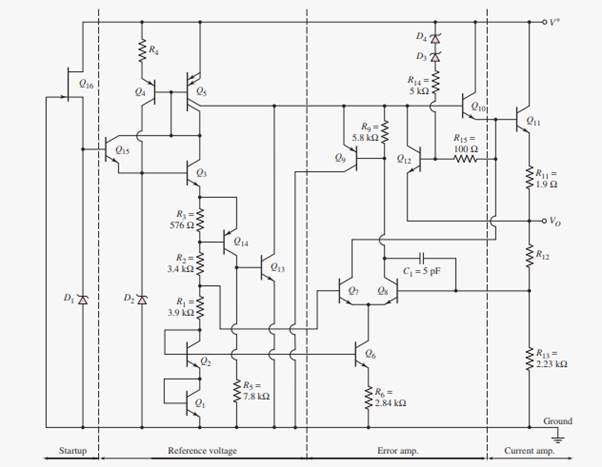
Circuit diagram for voltage regulator is shown below.
The voltage of Zener diode
Transistor parameters of
Also the resistor in the emitter of
The expression for bias current
Substituting 5.6 V for
The value of current
The expression for Emitter-base voltage of transistor
Also,
The expression for emitter-base voltage of transistor
Also,
The expression for emitter-base voltage of transistor
Substituting values of
Substituting value of
Let’s consider the current values 0.205 mA, 0.213 mA, and 0.220 mA for
Substituting values 0.213 mA for
Substituting again 0.220mA for
Hence, the current value 0.213mA is satisfying the equation (2)
After trial and error method it is found that the value of current
The reference voltage of temperature compensated portion (
Substitute 0.6 V for
Hence, the reference voltage of temperature compensated portion is 3.08 V.
(b)
Resistance
(b)
Answer to Problem 15.16EP
The value of resistance
Explanation of Solution
Given:
The voltage of Zener diode
Transistor parameters of
Also the resistor in the emitter of
Given voltage
The expression for reference voltage (
Here,
Let’s re-arrange above expression to find the resistance
Substituting
The value of resistance
Want to see more full solutions like this?
Chapter 15 Solutions
Microelectronics: Circuit Analysis and Design

- Two low pass signals, each band limited 4 KHz, are to be time multiplexed into a single channel using PAM. Each signal is impulse sampled at a rate 10 KHz. The time multiplexed signal waveform is filtered by an ideal LPF before transmission. (a) What is minimum clock frequency of the system? (b) What is the minimum cut off frequency of the LPF? Ans. (a) 20KHz (b) 10KHzarrow_forwardc. For the circuit shown in Figure, determine lc and VCB. Assume the transistor to be made of Silicon. Ic RE=1.6 kn Rc=1.1 kn EE=8 V Vcc= 20 varrow_forwardFind value of RT so that output voltage Vo is (-1.5)(volt).arrow_forward
- For these circuit finf the input impedanc Zi only .....arrow_forwardA collector modulator is a balanced modulator. True False The information or intelligence is at the sidebands. O True False The tank circuit is used to increase carrier frequency in the diode modulator. True O Falsearrow_forwardExplain construction and working principle of JFET. Also draw drain and transfer characteristics of a JFET.arrow_forward
- Q1: From the circuit shown below:- Vrms=19.8V f₁ =125Hz For the given circuit, a) State the name of each stage:- Stage 1 is Stage 2 is Stage 3 is Stage 1 is Stage 1 Stage 2 is Stage 3 is 0.5μF ...... ww Stage 2 R oscillator Ripple Filter Half Wave Rectifier Voltage Regulator b) The output plots below, match each stage with its output plot: (a) Voltage Regulator Full Wave Rectifier (c) (sec) Stage 3 Vout (b) (d) (sec) t mmmm (sec) (sec)arrow_forwardA Bipolar junction Transistor with curreat amplification factor being 100, Input Base current is 50μA. Collector voltage is 10 V and biasing voltage being +20 V. Find followings a. Collector current b. Resistance (R1) c. Collector voltage , Emitter voltage , Base Voltage & Collector-Emitter Voltage.arrow_forwardAssume R1= R2 =D6002, RL=500, and Vcc = 15V. Assuming D1 and D2 are identical and have same characteristics as Q1 and Q2 base-emitter junctions, if the input voltage is 1Vrms, what will be the output peak voltage? Vcc R1 D1 D2 Q2 R2 R2 -Vccarrow_forward
- The analog input channel voltage range for a PIC16 Microcontroller is limited to the positive range 0-Vref. Many situations require a digitized mapping from bipolar analog signals to unipolar signals. A simple resistive network has been designed to translate a bipolar voltage range of ±10V to a unipolar range of 0-6.6 V, assuming Vref is +6.6 V. A reasonable resistor combination is: a. None of them b. 2.212, 2.70, and 5 Kohms c. 2.212, 2.70, and 2.70 Kohms d. 1.122, 1.70, and 3.30 Kohmsarrow_forwardFill in the table VB VC VE Ic LE I8 fre IT gm 5V Consider the circuit given at the right. 600k 1.5k =0.7, Vauo, B=165) 100uF Vo 1k 100uF a) Perform DC analysis and calculate all VB =? VC:? branch currents, node voltages, and small signal parameters 3K VE=? Rout b) Draw a small-signal equivalent model n Vin Rin 400K c) Calculate Ri, Rout, and Ay=Vou/Vin -5Varrow_forwardDesign a buck-boost converter with the specifications: Vin = 28 V, in %3D the range [24V,32V], Vout=12 V (with opposite polarity to Vin), load power in the range [0, 120 W], such that to operate in CCM for any line and load value. Select a switching frequency of 100kHz. Choose C= 1.8mF, 25V, 2.5mQ.arrow_forward
 Introductory Circuit Analysis (13th Edition)Electrical EngineeringISBN:9780133923605Author:Robert L. BoylestadPublisher:PEARSON
 Delmar's Standard Textbook Of ElectricityElectrical EngineeringISBN:9781337900348Author:Stephen L. HermanPublisher:Cengage Learning
 Programmable Logic ControllersElectrical EngineeringISBN:9780073373843Author:Frank D. PetruzellaPublisher:McGraw-Hill Education
 Fundamentals of Electric CircuitsElectrical EngineeringISBN:9780078028229Author:Charles K Alexander, Matthew SadikuPublisher:McGraw-Hill Education
 Electric Circuits. (11th Edition)Electrical EngineeringISBN:9780134746968Author:James W. Nilsson, Susan RiedelPublisher:PEARSON
 Engineering ElectromagneticsElectrical EngineeringISBN:9780078028151Author:Hayt, William H. (william Hart), Jr, BUCK, John A.Publisher:Mcgraw-hill Education,