
Concept explainers
Videos
Consider the NMOS inverter with resistor load in Figure 16.3(a) biased at
(a)
The value of
Answer to Problem 16.1EP
The value of
Explanation of Solution
Given:
Calculation:
Consider the NMOS inverter with resister load biased at
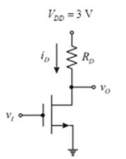
Figure 1
From the circuit,
Calculate the value of
Since,
The current drain equation is,
Apply Kirchhoff’s voltage law to the circuit.
Conclusion:
Therefore, the value of
(b)
The maximum current and maximum power dissipation in the inverter.
Answer to Problem 16.1EP
The maximum power transfer is,
The maximum drain current is,
Explanation of Solution
Given:
Calculation:
Consider Figure 1.
The maximum current is,
The maximum power transfer is,
Conclusion:
Therefore, the maximum power transfer is,
(c)
The transition point for the driver transistor.
Answer to Problem 16.1EP
The transition point for the driver transistor is
Explanation of Solution
Given:
Calculation:
Transitionpoints for the driver resistor is
As the transition voltage is positive and greater than zero for NMOS, the input transition voltage is
The output transition voltage is,
Conclusion:
Therefore, the transition point are
Want to see more full solutions like this?
Chapter 16 Solutions
Microelectronics: Circuit Analysis and Design


- 5) Design a linear suturated load inverter shown in the below figure with VDD= 3.3V,VL = 0.2V and P = 100µ W. Assume VTO= 0.6V, y = 0.6Vv, and 26F= 0.6V. %3D VGG = 6.0 V o 오 VDD ML o vo Ms Dr. Abdulla Abmed Rabeeaarrow_forwardThe load voltage waveform of a single phase full bridge inverter supplied from 300V DC voltage source is shown in below figure. Output frequency is 50HZ and the load consists of series R-L components. The load values are 22 and 0.04H, respectively. (Conduction interval for half period is 120°) 150 100 50 T -50 3 -100 -150 .002 .004 .006 .008 .01 .012 .014 .016 .018 .02 Time (sec) a. Calculate and draw the load current for the first two-period interval b. Calculate and draw the load current for the steady-state conditionarrow_forwardA full-bridge inverter has a switching sequence that produces a square wave voltage across a series RL load. The switching frequency is 60 Hz, Vdc=100 V, R10=Ohm, and L= 25 mH. The power absorbed by the load is. Select one: O a. None of the above O b. 1500 W O c. 1000 W O d. 441 Warrow_forward
- With a single phase full bridge square wave inverter connected to a 24V DC power supply, 50H output frequency AC output is aimed. The load resistance is 10 ohms and the inductor is 250mH. Calculate the maximum value (in milliamps) of the load current. a) 546 b) 474 c) -546 d) -474 e) 323arrow_forwardA single phase bridge inverter has an RLC load with R= 20 ohms. L = 32 mH and C = 0.115 mF. The inverter frequency is fo= 60 Hz and DC input voltage is Vs = 110 V. The RMS magnitude of the 1st harmonic of the output current is equal to: Select one: a. 4.34A b. 6.42A OC. 0.955A Qd. None of thesearrow_forwardAn inverter with a resistive load, VDD = 3.3 V, P = 0.1 mW, VL = 0.2 V, K'n = 60 UA/V2 and VT N = 0.75 V. The value of (W/L)S is:arrow_forward
- The load voltage waveform of a single phase full bridge inverter supplied from 300V DC voltage source is shown in below figure. Output frequency is 50HZ and the load consists of series R-L components. The load values are 2N and 0.04H, respectively. (Conduction interval for half period is 120°) 150 100 50 T -50 3 -100 -150 .002 .004 .006 .008 .014 ,02 .01 Time (sec) .012 .016 .018 a. Find the RMS values of the load voltage and the load current b. Calculate and draw the voltage across the load inductance c. Calculate and draw the source current and find its average valuearrow_forward4. Consider the circuit below on the left. a) What logic function does it perform? (What is F in terms of inputs A and B?) b) Find the transistor sizes (NMOS and PMOS widths) so that the fundamental dynamics are that of the symmetrical inverter on the right. VDD Ā- A - B 6W F 3W A Вarrow_forwardElectrical Engineering For the ECL inverter shown in the following sketch, the high voltage level is VH = -1.7V and the average power dissipated when the input is high 50% of the time is P = 5mW. Determine the source's current IEE, the low voltage level V, the reference voltage level VREF and the value of resistance R3. 2kQ 2k2 VREF EE -3.3V -5.2Varrow_forward
- a) Design an NMOC inverter with a resistive load (Find the value of R and W/L) for VDD = 5 V andP = 0.2 mW with V1 = 0.15 V. Assume Kn' = 60µA/V² and VTN = 0.7V. b) Find the noise margins associated with the designed inverter. c) Verify your design with PSPICE or Multisim. VDD R o vo ip Ms UDS R = W/L = VH = Ipp VL Calculated or (Given) Simulatedarrow_forward1. A square-wave inverter has an R-L load with R=15 Ω and L=10 mH. The inverter output frequency is400 Hz (fundamental frequency).(a) Determine the values of the required to establish a load current which has a fundamentalfrequency component of 10 A rms with α = 0.(b) For a controlled full-bridge inverter, the dc source is 125 V and the switching frequency is60 Hz. Determine the value of α to produce an output with amplitude of 100 V at the fundamentalfrequency.arrow_forwardA CMOS inverter has VDD = 1.8 V, Vtn = 0.5 V, and Kn = µnɛox/2Tox = 125 µA/V?. The ITC for this inverter is plotted below. What is W/L of the nMOS transistor? 2. 3.0е-4 2.5e-4 2.0e-4 1.5e-4 1.0е-4 5.0e-5 0.0e+0 0 0.2 0.4 0.6 0.8 1.0 1.2 1.4 1.6 1.8 Vin (V) IDD (A)arrow_forward
 Introductory Circuit Analysis (13th Edition)Electrical EngineeringISBN:9780133923605Author:Robert L. BoylestadPublisher:PEARSON
 Delmar's Standard Textbook Of ElectricityElectrical EngineeringISBN:9781337900348Author:Stephen L. HermanPublisher:Cengage Learning
 Programmable Logic ControllersElectrical EngineeringISBN:9780073373843Author:Frank D. PetruzellaPublisher:McGraw-Hill Education
 Fundamentals of Electric CircuitsElectrical EngineeringISBN:9780078028229Author:Charles K Alexander, Matthew SadikuPublisher:McGraw-Hill Education
 Electric Circuits. (11th Edition)Electrical EngineeringISBN:9780134746968Author:James W. Nilsson, Susan RiedelPublisher:PEARSON
 Engineering ElectromagneticsElectrical EngineeringISBN:9780078028151Author:Hayt, William H. (william Hart), Jr, BUCK, John A.Publisher:Mcgraw-hill Education,