
Videos
All parameters associated with the instrumentation amplifier in Figure 9.26are the same as given in Exercise Ex 9.8, except that resistor
The value of maximum common mode gain.
Answer to Problem 9.72P
The maximum value of the voltage gain is
Explanation of Solution
Calculation:
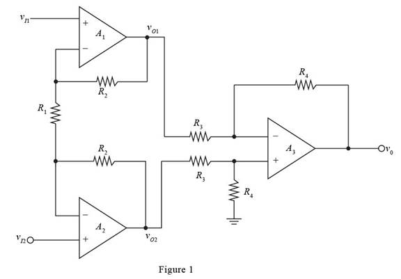
The given diagram is shown in Figure 1
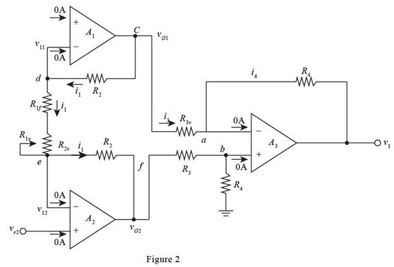
Mark the voltages and current and redraw the circuit.
The required diagram is shown in Figure 2
The expression for the voltage
The expression for the current at the node
Substitute
Apply KCL at the node
Substitute
The expression for the value of the current
The expression for the voltage
Substitute
The expression for the voltage
Substitute
Substitute
The expression for the common mode voltage is given by,
The expression for the differential voltage is given by,
The expression for the voltage
The expression for the voltage
Substitute
The general expression for the output equation is given by,
From above and from equation (3), the expression for the common mode gain is evaluated as,
Substitute
From above the range of the common mode voltage gain is given by,
The maximum value of the voltage gain is given by,
Conclusion:
Therefore, themaximum value of the voltage gain is
Want to see more full solutions like this?
Chapter 9 Solutions
Microelectronics: Circuit Analysis and Design


- what is the Ad gain for the following diferrential amplifier (see attached figure).arrow_forwardQ2// Answer the following questions about voltage-feedback bias circuit for the figure below. 1-Determine Ver and VCB. 2- What happens to the voltage Ve if the resistor Rp is open? 22 K 3- What might cause VCE to become nearly 9 V? 4- Determine the change in Ie from 25° to 75° C, if Ico 0.2 HA, and VBE = 0.7V. 10 ul B-80arrow_forward3. A simple current bias reference circuit based on the base-emitter junction voltage is depicted in Figure 9.3. Determine the sensitivity S of the output current to supply voltage Vcc. It is given that Is = 5 x 10-15A and assume that VT = 26 mV. (Hint: Assume that Vcc >> VBE(on) and use this to simplify the calculation.) Vcc= 15 V I R₁ Q₁ 10 ΚΩ 22 J R₂ 1 ksz Figure 9.3arrow_forward
- 10. Refer to the JFET transfer characteristic curve in Figure 9–16(a) and determine the peak-to- peak value of I, when Ves is varied ±1.5 V about its Q-point value.arrow_forwardA voltage follower is to be designed to provide a gain error of less than 0.005 percent. Develop a set of minimum required specifications on open-loop gain and CMRR.arrow_forwarda- Zero. b- Slightly different from zero. O Maximum positive or negative. d- An amplified sin wave. 9-Negative feedback reduces @ The feedback fraction. b- Distortion. c- The input offset voltage. d- The open-loop gain. 10-The input impedance of a current-voltage converter is Small. b- Large. c- Ideally zero. d- Ideally infinite. a- 11-In a linear op-amp circuit, the @ Signal are always sin wave. b- Op-amp does not go into saturation. c- Input impedance is ideally infinite. d- Gain-bandwidth product is constant.arrow_forward
- 9- Results and Discussion:- 1-what are the differences between the inverting and non-inverting operation amplifier? 2- The output signal of the inverting amplifier is out of phase with its input signal by a) 0° b)90° c)180° d)270° 3-what are the differences between the integrator and differentiator operation amplifier? 4-lf a triangle waveform is applied to the differentiator circuit. What is the output signal will be?arrow_forward1- Mention any two advantages of Integrated Circuit . 2- For the circuit given below : Vin is a sine wave Vinpp=6 V and Vref=-2.4 V , Assume Vsat=±12V Name the circuit and draw the input and output waveforms . Vin Vref 3- Explain why open-loop op-amp configurations are not used in linear applications? Draw the block diagram of opamp and define the function of each blockarrow_forwardare 9.16 The parameters of the two inverting op-amp circuits connected in cascade in Figure P9.16 R₁ = 10 ks2, R₂ = 80 ks, R3 = 20 k2, and R4 = 100 ks2. For v = -0.15 V, determine voi, vo, 11, 12, 13, and i4. Also determine the current into or out of the output terminal of each op-amp. R₁ V10- ww 7₁ Figure P9.16 R₂ www + 201 R3 ww 13 R₁ ww is -000arrow_forward
 Introductory Circuit Analysis (13th Edition)Electrical EngineeringISBN:9780133923605Author:Robert L. BoylestadPublisher:PEARSON
 Delmar's Standard Textbook Of ElectricityElectrical EngineeringISBN:9781337900348Author:Stephen L. HermanPublisher:Cengage Learning
 Programmable Logic ControllersElectrical EngineeringISBN:9780073373843Author:Frank D. PetruzellaPublisher:McGraw-Hill Education
 Fundamentals of Electric CircuitsElectrical EngineeringISBN:9780078028229Author:Charles K Alexander, Matthew SadikuPublisher:McGraw-Hill Education
 Electric Circuits. (11th Edition)Electrical EngineeringISBN:9780134746968Author:James W. Nilsson, Susan RiedelPublisher:PEARSON
 Engineering ElectromagneticsElectrical EngineeringISBN:9780078028151Author:Hayt, William H. (william Hart), Jr, BUCK, John A.Publisher:Mcgraw-hill Education,