
(a)
Interpretation:
The given material
Concept introduction:
Semiconductor: A material which can conduct electricity in range between a metal and an insulator is known as semiconductor. Addition of small amount of impurities increases conductivity of semiconductor and the process is known as doping. n-type and p-type are two types of doped semiconductors.
n-type: This is a type of doped semiconductor in which many free electrons are present in conduction band.
p-type: This is a type of doped semiconductor in which holes are present in valance band.
Insulator: Insulators are one, in which electrons are filled in valence band with a vacant conduction band and they are parted away by band gap.
Conductor: Any material which can conduct electricity is known as conductor. There will be no band gap in metallic conductor and electrons can easily travel.
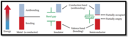
Figure 1
h
(b)
Semiconductor: A material which can conduct electricity in range between a metal and an insulator is known as semiconductor. Addition of small amount of impurities increases conductivity of semiconductor and the process is known as doping. n-type and p-type are two types of doped semiconductors.
n-type: This is a type of doped semiconductor in which many free electrons are present in conduction band.
p-type: This is a type of doped semiconductor in which holes are present in valance band.
Insulator: Insulators are one, in which electrons are filled in valence band with a vacant conduction band and they are parted away by band gap.
Conductor: Any material which can conduct electricity is known as conductor. There will be no band gap in metallic conductor and electrons can easily travel.
Figure 1
(c)
Interpretation:
The given material white tin has to be classified as a metallic conductor or an n-type semiconductor or a p-type semiconductor and or an insulator.
Concept introduction:
Semiconductor: A material which can conduct electricity in range between a metal and an insulator is known as semiconductor. Addition of small amount of impurities increases conductivity of semiconductor and the process is known as doping. n-type and p-type are two types of doped semiconductors.
n-type: This is a type of doped semiconductor in which many free electrons are present in conduction band.
p-type: This is a type of doped semiconductor in which holes are present in valance band.
Insulator: Insulators are one, in which electrons are filled in valence band with a vacant conduction band and they are parted away by band gap.
Conductor: Any material which can conduct electricity is known as conductor. There will be no band gap in metallic conductor and electrons can easily travel.
Figure 1
(d)
Interpretation:
The given material germanium doped with gallium has to be classified as a metallic conductor or an n-type semiconductor or a p-type semiconductor and or an insulator.
Concept introduction:
Semiconductor: A material which can conduct electricity in range between a metal and an insulator is known as semiconductor. Addition of small amount of impurities increases conductivity of semiconductor and the process is known as doping. n-type and p-type are two types of doped semiconductors.
n-type: This is a type of doped semiconductor in which many free electrons are present in conduction band.
p-type: This is a type of doped semiconductor in which holes are present in valance band.
Insulator: Insulators are one, in which electrons are filled in valence band with a vacant conduction band and they are parted away by band gap.
Conductor: Any material which can conduct electricity is known as conductor. There will be no band gap in metallic conductor and electrons can easily travel.
Figure 1
(e)
Interpretation:
The given material stainless steel has to be classified as a metallic conductor or an n-type semiconductor or a p-type semiconductor and or an insulator.
Concept introduction:
Semiconductor: A material which can conduct electricity in range between a metal and an insulator is known as semiconductor. Addition of small amount of impurities increases conductivity of semiconductor and the process is known as doping. n-type and p-type are two types of doped semiconductors.
n-type: This is a type of doped semiconductor in which many free electrons are present in conduction band.
p-type: This is a type of doped semiconductor in which holes are present in conduction band.
Insulator: Insulators are one, in which electrons are filled in valence band with a vacant conduction band and they are parted away by band gap.
Conductor: Any material which can conduct electricity is known as conductor. There will be no band gap in metallic conductor and electrons can easily travel.
Figure 1
Want to see the full answer?
Check out a sample textbook solution
Chapter 21 Solutions
General Chemistry: Atoms First

- 8.96 A business manager wants to provide a wider range of p- and n-type semiconductors as a strategy to enhance sales. You are the lead materials engineer assigned to communicate with this manager. How would you explain why there are more ways to build a p-type semiconductor from silicon than there are ways to build an n-type semiconductor from silicon?arrow_forwardClassify as n-type or p-type a semiconductor formed by doping (a) germanium with phosphorus, (b) germanium with indium.arrow_forwardThe maximum wavelength of light that a certain silicon photocell can detect is 1.11 μm. (a) What is the energy gap (in electron volts) between the valence and conduction bands for this photocell? (b) Explain why pure silicon is opaque.arrow_forward
- Define a semiconductor? Describe the two main types of semiconductorswhen it is doped with(a) group 13 element, (b) group 15 element.arrow_forwardThe lead(IV) oxide used in car batteries is prepared by coat-ing the electrode plate with PbO and then oxidizing it to leaddioxide (PbO₂). Despite its name, PbO₂ has a nonstoichiometricratio of lead to oxygen of about 1/1.98. In fact, the holes in the PbO₂ crystal structure due to missing O atoms are responsiblefor the oxide’s conductivity. (a) What is the mole % of O miss-ing from the PbO₂ structure? (b) What is the molar mass of the nonstoichiometric compound?arrow_forwardWhich of the following alloys does not contain copper? (A) Bronze (B) Pewter (C) Sterling silver (D) None of themarrow_forward
- Which of these statements is false?(a) As you go down column 4A in the periodic table, the elementalsolids become more electrically conducting. (b) Asyou go down column 4A in the periodic table, the band gapsof the elemental solids decrease. (c) The valence electroncount for a compound semiconductor averages out to fourper atom. (d) Band gap energies of semiconductors rangefrom ∼0.1 to 3.5 eV. (e) In general, the more polar the bondsare in compound semiconductors, the smaller the band gap.arrow_forwardSome oxide superconductors adopt a crystal structure similar to that of perovskite (CaTiO3). The unit cell is cubic with a Ti4+ ion in each corner, a Ca2+ ion in the body center, and O2- ions at the midpoint of each edge. (a) Is this unit cell simple, body-centered, or face-centered? (b) If the unit cell edge length is 3.84 Å, what is the density of perovskite (in g/cm3)?arrow_forwardAccount for the relative band gap energies of semiconductors interms of periodic trends?arrow_forward
 Chemistry for Engineering StudentsChemistryISBN:9781337398909Author:Lawrence S. Brown, Tom HolmePublisher:Cengage Learning
 Principles of Modern ChemistryChemistryISBN:9781305079113Author:David W. Oxtoby, H. Pat Gillis, Laurie J. ButlerPublisher:Cengage Learning
 Chemistry: Principles and PracticeChemistryISBN:9780534420123Author:Daniel L. Reger, Scott R. Goode, David W. Ball, Edward MercerPublisher:Cengage Learning